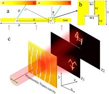
Controlling both amplitude and phase of light in the subwavelength scale is a challenge for traditional optical devices. Here, we propose and numerically investigate a novel plasmonic meta-hologram, demonstrating broadband manipulation of both phase and amplitude in the subwavelength scale. In the meta-hologram, phase modulation is achieved by the detour phase distribution of unit cells, and amplitude is continuously modulated by a T-shaped nano-cavity with tunable plasmonic resonance. Compared to phase-only holograms, such a meta-hologram could reconstruct three-dimensional (3D) images with higher signal-to-noise ratio and better image quality, thus offering great potential in applications such as 3D displays, optical communications, and beam shaping.
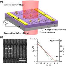
Monitoring the chemical and structural changes in protein side chains and endpoints by infrared (IR) spectroscopy is important for studying the chemical reaction and physical adsorption process of proteins. However, the detection of side chains and endpoints in nanoscale proteins is still challenging due to its weak IR response. Here, by designing a double layered graphene plasmon sensor on MgF2/Si substrate in the IR fingerprint region, we detect the vibrational modes in side chains and endpoints (1397 cm 1 and 1458 cm 1) of monolayer protein. The sensor could be applied on biochemistry to investigate the physical and chemical reaction of biomolecules.
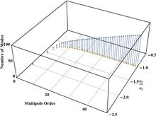
In the context of nonlinear plasmonics, we review the recently introduced concept of plasmonic parametric resonance (PPR) and discuss potential applications of such phenomena. PPR arises from the temporal modulation of one or more of the parameters governing the dynamics of a plasmonic system and can lead to the amplification of high-order sub-radiant plasmonic modes. The theory of PPR is reviewed, possible schemes of implementation are proposed, and applications in optical limiting are discussed.
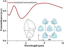
A gradient-index Reuleaux-triangle-shaped hole array was fabricated on germanium (Ge) by nanoimprint lithography and inductively coupled plasma processing as a broadband mid-infrared (IR) antireflective surface. The interaction between the {111} planes of cubic crystalline Ge and a circular mold successfully produced an orderly and periodically distributed Reuleaux-triangle-shaped hole array. As a result, the average transmittance increased 15.67% over the waveband at 3–12 μm and remained stable at the incidence angle of up to 60°. The vertices of the Reuleaux triangle showed local enhancement of the electric field intensities due to interference of the incident and reflected radiation fields. It was also found that nonuniform hole depths acted to modulate the transmittance over the 3–12 μm waveband.
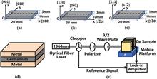
In this Letter, we have demonstrated significant electric field induced (EFI) optical rectification (OR) effects existing in the surface layers of germanium (Ge) and measured the distributions of EFI OR signals along the normal directions of surface layers of Ge samples. Based on the experimental results, the ratios of the two effective second-order susceptibility components χzzz(2eff)/χzxx(2eff) for Ge(001), Ge(110), and Ge(111) surface layers can be estimated to be about 0.92, 0.91, and 1.07, respectively. The results indicate that the EFI OR can be used for analyzing the properties on surface layers of Ge, which has potential applications in Ge photonics and optoelectronics.
Higher emission rates and controllable emission direction are big concerns when it comes to finding a good single photon source. Recently, surface plasmons are introduced to this application, as they can manipulate and enhance the luminescence of single emitters. Here, we experimentally achieve a wide-area multiple directional enhanced light source through periodic metal grating structures. The surface-plasmon-coupled emission can have multiple precisely emission angles by just changing the period of the grating. Our result indicates that metal plasmonic grating can be used as a productive quantum device for unidirectional quantum light sources in quantum optics.
The depth profile of electric-field-induced (EFI) optical rectification (OR) and EFI Pockels effect (PE) in a Si(110) crystal are investigated. The results show that EFI OR and PE signals are very sensitive to the electric field strength in the surface layers of the Si crystal. Theoretical formulas that include the electric field parameters and the widths of the space-charge region are presented and agreed very well with the experimental results. The experiments and simulations indicate that EFI OR and PE are potential methods for researching the surface/interface properties along the depth direction in centrosymmetric crystals such as Si.
The spin Hall effect of light (SHEL) can be observed by the dark strip resulting from weak measurement. We find that the SHEL of a partially coherent beam (PCB) has a similar phenomenon as well. However, the dark strip in the SHEL of a PCB cannot be explained by considering the beam as an assemblance of coherent speckles. Also, the dark strip in a PCB is not purely dark. By analyzing the autocorrelation, we show that the SHEL of a PCB is the result of overlapping coherent speckles’ SHEL. We further prove our conclusion by adjusting convergence and incident angles. Finally, we develop a qualitative theory to clarify the SHEL of a PCB.
A terahertz (THz) waveguide using a metallic nanoslit whose width is much smaller than the skin depth is analytically investigated. By taking some important physical properties into account, we derive a simple, yet accurate, expression for the effective index. We also study the changes in modal field and the attenuation coefficient in the whole THz region, and find some interesting physical properties. Finally, we verify that these theoretical analyses coincide with the rigorous numerical simulations. This research can be useful for various applications of THz waveguides made of metallic nanoslits.
We experimentally investigate the effects of the surface roughness of gold thin films on the properties of surface plasmon resonance. By annealing at different temperatures, film samples with different surface morphologies are obtained. Specifically, due to the diffusion of the gold atoms towards the films’ surface, the surface root-mean-square roughness decreases with the increasing annealing temperature. Then, we measure the surface plasmon resonance of the samples. The results show that the resonance angle of the surface plasmon resonance is sensitive to the root-mean-square roughness, and it gradually decreases by reducing the surface root-mean-square roughness.
In this study, a new method utilizing surface plasmon resonance (SPR) sensing technology based on the phase and angular interrogations for measuring the refractive index of a liquid prism is presented. An orthogonal sample box that combined the functions of a prism, cell box, and mirror is adopted to simplify the system and provide the convenience to implement the phase and angular interrogations. The angular interrogation is achieved by the motorized rotation stage with the new sample box, and the phase interrogation is achieved by the linear polarization interferometry between the s- and p-polarization components. The amplitude reflectivity and the phase angle, which are the functions of the incident angle, are obtained by the reflection intensity and the interference intensity of the lights directly. A sensitivity of 7.5×10 7 refractive index unit (RIU)/0.1° and a dynamic range of 0.5 RIU are obtained experimentally and theoretically.
The advantages of manufacturing a space aspheric mirror of SiC material are analyzed, and the key methods and technology of fabricating and measuring SiC aspheric surfaces are introduced and researched. The off-axis SiC aspheric mirror is ground and polished by computer controlled optical surfacing (CCOS) technology with a FSGJ-2 numerical control machine, the contour and optical parameters are measured and controlled by a coordinate measuring machine (CMM) and laser tracker. Finally, an example for fabricating and testing an off-axis parabolic mirror with an aperture of 820 mm is given. A null lens is specifically designed and customized in order to test the large aspheric mirror by interferometry and null compensation. The resulting PV and RMS of the surface error are 0.335λ and 0.018λ (λ is 632.8 nm), respectively, which meets the requirements of the optical design.
We theoretically study the nonlinear surface wave propagation at the interface between superconductor media and nonlinear metamaterials. The dispersion equation is analytically derived and solved numerically. Moreover, we present the power for the propagating waves at the interface. The results display different behaviors of the propagating waves as the nonlinear term or temperature is tuned. These results indicate that this structure can have potential applications in superconductor waveguide devices and integrated optics.
We propose a scheme to obtain a low-loss propagation of Airy surface plasmon polaritons (SPPs) along the interface between a dielectric and a negative-index metamaterial (NIMM). We show that by using the transverse-magnetic mode and the related destructive interference effect between electric and magnetic absorption responses, the propagation loss of the Airy SPPs can be largely suppressed when the optical frequency is close to the lossless point of the NIMM. As a result, the Airy SPPs obtained in our scheme can propagate more than a 6 times longer distance than that in conventional dielectric–metal interfaces.
A model that considers both thermal expansion and thermo-optical effects is developed to investigate the transmission variation of optical coatings when they are exposed to an intense laser beam. Our results indicate that a higher gradient of the transmission spectrum curve at a certain wavelength leads to a more evident variation of the coating transmission. Three customized HfO2–SiO2 multilayer coatings with different transmission spectra are used to measure the transmitted power under the irradiation of a 1080 nm continuous-fiber laser. Excellent agreement is found between the experimental result and the theoretical prediction. Our result is helpful for the improvement of such devices in the application of high-power laser systems.
In this Letter, silver (Ag) hierarchical nanostructures grown on black silicon (BS) are used as the catalyst and a surface-enhanced Raman scattering (SERS) detector integrated in a microfluid. The BS is fabricated via femtosecond laser ablation in an atmosphere of sulfur hexafluoride, and then hydrogenated with hydrofluoric acid. As formed, the BS substrate directly acts as a reducing template to grow silver hierarchical nano-structures. Particularly, Ag-BS composite micro/nano-structures can be in-situ constructed in silicon-based microchannels. These structures simultaneously serve as integrated catalytic reactors and a SERS substrate for sensing. The sensitivity is tested to be as low as 10 8 mol/L using Rhodamine 6G.
We study all-optical sensing characteristics based on long-range surface plasmon resonance in a four-layered metal-dielectric structure immersed in the liquid to be measured. The resonance peaks in the reflection angle spectra depend on different refractive indices from 1.30 to 1.38, which are calculated and compared in three typical wavelengths of 532, 632.8 and 780 nm, respectively. Compared with 532 nm, the incident light of 780 nm results in an unstable sensing stability, but the resolution enhances two times. The sensitivity of this refractive index sensor at an incident angle of 45° is about 236.7 nm/RIU which uses 532-nm laser as the light source.
A porous silicon microcavity (PSM) is highly sensitive for sensing applications due to its high surface area and a narrow resonance peak. In this letter, we fabricated the PSM by alternate current density from a low value to a high value during double-tank electrochemical anodization at different electrolyte temperatures. Results show that with the increase of the electrolyte temperature, the rate of the PS etching becomes faster and the refractive index of the PS layer becomes smaller. The thickness of the PS increases faster than the decrease of the refractive index of the PS.
A simple, low-cost, and high-efficient method is used for the fabrication of surface-enhanced Raman scattering (SERS) substrates. Silver particles deposited on porous silicon are prepared as a highly efficient SERS substrate by direct immersion of porous silicon in silver solution. The SERS measured with rhodamine 6G as a target molecule is affected by the morphology of silver particles on the top of porous silicon layer. The effect of solution concentration, dipping time, and thickness of porous layer on the morphology of silver particle is investigated. Highly efficient SERS spectra are observed for substrates with porous layer thickness of about 3 μm and incubated in the 50 mM AgNO3 solution for 3 minutes. The SEM images of the substrates show that there are many small Ag particles with the size of a few nanometers among large Ag particles with the size of several microns.
We propose and analyze a long-range dielectric-loaded surface plasmon polariton (SPP) waveguide based on graded-index ridge over server millimeter distances. Then the influence of the dielectric thickness and the ridge refractive index on propagation length and mode width is discussed and simulated with the finite ele-ment method. The result shows that the SPP can propagate as long as 3.42 mm, as well as the mode width keeping as 1.64 mm, a better one compared with the fixed refractive index. Considering its nanoscale dimen-sion and outstanding performance, the structure is easily realized when connected with electrodes.
High-sensitivity and broad bandwidth photo-detector devices are important for both fundamental studies and high-technology applications. Here, by using three-dimensional (3D) finite-difference time-domain simulation, we design an optimized 3D multilayer gold nano-antenna to enhance the nearinfrared (NIR) absorption of germanium nanoparticles. The key ingredient is the simultaneous presence of multiple plasmonic resonance modes with strong light-harvesting effect that encompass a broad bandwidth of germanium absorption band. The simulation results show more than two orders of magnitude enhanced absorption efficiency of germanium around 1550 nm. The design opens up a promising way to build high-sensitivity and broad bandwidth NIR photo-detectors.
We present an experimental study on a unidirectional surface plasmon polariton (SPP) launcher based on a compact binary area-coded nanohole array, where the symmetry breaking is realized via effective-index modulation in the binary pattern of the gold film, thus avoiding the challenge of modulating nanostructure in its depth. It is shown that SPPs can be unidirectionally and effectively excited at normal incidence. The SPP intensity and asymmetric excitation ratio, which are two key figure-of-merits of SPP launchers, can be improved by increasing the number of array rows. The proposed device is compatible with most mature top-town nanofabrication techniques and thus is perspective for low-cost mass production.
Spin (polarization) is widely used in free-space optics, while in photonic integrated circuits (PICs), information is usually encoded in optical route. So a practical way to connect these two encoding methods is necessary for information communication. In this letter, an encoding convertor is designed to connect spin encoding and route encoding. Finite element method is used to calculate the conversion efficiency and extinction ratio of the encoding convertor and the theoretical analyses are also given. Our protocol shows a friendly way to convert optical spin information to route information, which will promote the compatibility of free-space optics and PICs.
We propose new types of hybrid plasmonic waveguides for low-threshold nanolaser applications. Modal properties and lasing threshold under different geometric shapes and parameters are investigated and -analyzed by the finite element method, aiming to realize both low propagation and high field confinement. Results show that a smaller gap width and a larger round corner radius of the metal film reduce the lasing threshold. These new structures can open up new avenues in the fields of active plasmonic circuits.
A new plasmonic nanolens that can be tuned by varying the circular structure into an elliptical annulus and the aspect ratio from 1 to 0.1 and 1 to 2, respectively, is proposed. Using the rigorous finite-difference and time-domain algorithm, we find that when the aspect ratio ranges from 1 to 0.1, a good linear relationship exists between the aspect ratio and focusing spot size at the full-width at half-maximum in the x- and y-directions, respectively. The corresponding calculated FWHM ranges from 96 × 126 (nm) to 15 \times 52 (nm) (Full Width at Half Maximum).
A structure which consists of photoresist film sandwiched by Ag nano-particle and metal film is proposed to modify localized hotspot both in transversal and longitudinal direction. It shows that there is strong plasmonic coupling between Ag nano-particle and metallic surface, which helps to reduce the width and elongate the depth of the plasmonic hotspot localized inside photoresist film. And that fringes and side lobes around hotspots can be effective attenuated by bottom-side illumination. Influences of illumination, particles inter-space, and polarization are also studied. The method opens avenue for the potential applications such as lithography, optical storage, etc.
Global change in the dispersive behavior of terahertz (THz) plasmons on metal wires with wide radii ranging from 5 nm to 0.5 mm is systematically investigated. Through rigorous numerical calculations, we find that the dispersion of a metal wire with a radius of 5 nm increases by about 4-6 orders of magnitude compared with the case of a metallic wire with a radius of 0.5 mm. Zero-dispersion points appear when the frequency is lower than 3 THz, and the positions of the zero-dispersion points can shift with the frequency. Finally, we provide an explicit expression that agrees very well with the numerical calculations.
The optical properties and plasmon resonance coupling of double coaxial gold nanotube arrays are investigated. The results show that the optical transmission is highly tunable by varying the thicknesses of the inner and outer nanotubes, the separation between the inner and outer nanotubes, and the dielectric parameters inside, between, and outside the two nanotubes. The shorter-wavelength transmission bands are very sensitive to the modification of the wall thickness of the outer nanotube, the separation, and the dielectric parameters between the double nanotubes. The dipole and multipolar plasmon modes are excited in our model. However, for small separation and refractive index, the dipole normal mode has a leading function in the transmission properties. Compared with the dipolar modes, the contribution of higher-order modes becomes larger as the parameters increase.
Surface-plasmon (SP) enhancement of amorphous-silicon-nitride (a-SiNx) light emission with single-layer gold (Au) waveguides is experimentally demonstrated through time-resolved photoluminescence measurement. The a-SiNx active layer with strong steady-state photoluminescence at 560 nm is prepared by plasma-enhanced chemical vapor deposition, and the Au waveguide on the top of the a-SiNx layer is fabricated by magnetron sputtering. The maximum Purcell factor value of ~3 is achieved with identified SP resonance of the Au waveguide at ~530 nm.
A novel plasmonic waveguide filter design based on three cascaded slot cavities is proposed. The cascaded nanocavities support a united resonant (UR) mode. Light is trapped in the middle nanocavity at telecommunication wavelength (1550 nm) when the UR mode exists. This phenomenon leads to the efficient transmittance and high Q factor of the plasmonic filter. The resonant wavelength and Q factor can be easily modulated by the cavity radii and the waveguide width.
We propose a surface plasmon resonance (SPR) sensor based on phase modulation and polarization interferometry, both of which provide a refractive index (RI) resolution of the same order as that of SPR sensors of the phase type. And it has a wide dynamic range and insensitivity of RI resolution to the thickness of metal films as that of the intensity type SPR sensors. In this letter, we choose electro-optic (EO) phase modulation instead of the angle modulation. We demonstrate theoretically that with the EO phase modulation, our sensor could provide a better RI resolution.
We present a design for tunable directional beaming through a subwavelength metallic double slit surrounded by dielectric surface-relief gratings. On-axis and off-axis beaming can be switched by controlling the incident angle to asymmetrically excite surface plasmon polaritons (SPPs) that are subsequently coupled out to propagating beams by the two gratings on the left and the right sides of the double slit. Furthermore, the division of optical power into two off-axis beaming directions can be tuned smoothly by varying the incident angle while keeping the total power almost unchanged. The mechanism of this effect is analyzed theoretically and verified using rigorous numerical simulations.
Road pavement reflectance is usually assumed to be invariant in short periods of time in some quantitative remote sensing applications. To examine its variability, reflectance sequences of concrete and asphalt pavement are measured in field for half a day in visible and near-infarecd (VNIR) spectral range using dual-beam method. As much as 20.7% and 3.52% of relative changes are found in asphalt and concrete reflectance data at 550 nm, and all VNIR bands demonstrate similar variations found to correlate with both illumination geometry and the relative portion of diffuse irradiance. In this letter, this effect is interpreted from a mathematic view. Further studies are needed to model the dynamics of reflectance physically.
As an employment of surface plasmonic effect, the consequence of insertion of a layer of Ag clusters into polymer solar cell on the enhancement of light absorption and power conversion efficiency is investigated. Optical analysis based on the finite-difference time-domain (FDTD) is performed with experiments to evaluate the effect of the interaction between the Ag clusters and incident light on light absorption in polymer solar cell. Ag clusters modify the light wave vector and the electromagnetic field inside the device is redistributed and enhanced. As a result, polymer solar cells achieve an overall increase in absorption, short-circuit current density, and power conversion efficiency.
Amino-functionalized mesoporous silica thin films (MTFs) are produced using surface active agent F127, and then gold nanoparticles are introduced into the pore channels to prepare the Au/SiO2 nanocomposite. After assembling the gold, the amino-functionalized MTF undergoes some shrinkage but remains a periodic structure as demonstrated by X-ray diffraction (XRD) patterns. The nanocomposite shows an acute characteristic diffraction peak assigned to (111) plane of the face-centered-cubic structure of gold, indicating that gold nanoparticles crystallize well and grow in a preferred orientation in the pore channels. The surface plasma resonance (SPR) absorption peak near 570 nm undergoes a red-shift accompanied by a strengthening of intensity when HAuCl4 is used to react with the amino groups on the internal pore surfaces for 4, 6, and 8 h. The simulative results are consistent with the experimental ones shows that the absorption property of the Au/SiO2 nanocomposite is influenced by the dipping time, which affects the size and volume fraction of embedded gold nanoparticles.


